TVS-Transient Voltage Suppressor Diode(2)
· Package
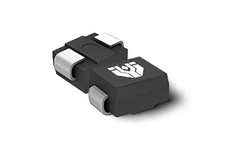
Because TVS needs to dissipate a significant amount of energy, the physical size needs to be larger. Common packages: DO-214, DO-218, DO-15, etc.
· Peak Pulse Power Dissipation
It indicates the capability to dissipate the maximum energy, with the testing condition specified as a 10/1000µs waveform. This means that this metric is a specific testing methodology within the industry and is not arbitrarily added with DC testing.
· Peak Pulse Curren
It indicates the ability to withstand the maximum pulse current. If this current is exceeded, there is a high likelihood that the TVS may become damaged.
· Peak Forward Surge Current
It refers to the maximum positive surge current magnitude. However, please note the testing conditions: 8.3ms Single Half Sine Wave. This means it is not a direct current, but rather a waveform with a very short duration.
· Parasitic capacitance
The parasitic capacitance is a parameter that can impact the practical application of TVS. In the case of data lines, it may result in changes to the data signal if the parasitic capacitance is too large
· Parasitic inductance
Parasitic inductance can impede the variation of high-frequency signals. Therefore, in the presence of high-frequency overcurrent/overvoltage pulses, if the parasitic inductance of the TVS is too large, it will significantly affect the protective effectiveness of the device.
· Leakage current
When a voltage is applied across the terminals of any material, there will be leakage current. If the leakage current is excessive, it can significantly impact the device's lifespan and increase the standby power consumption of the product.
·Breakdown Voltage
When a voltage is applied across the terminals of any material, there will be leakage current. If the leakage current is excessive, it can significantly impact the device's lifespan and increase the standby power consumption of the product.
· Reverse Stand-Off Voltage
VRWM, this parameter represents the voltage that should be applied across the terminals of the TVS when the device is operating normally. Under this voltage, the device will not trigger protective actions, and only a slight leakage current will flow.


评论
发表评论