博文

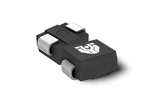
TVS-Transient Voltage Suppressor Diode(2)

图片
·  Package Because TVS needs to dissipate a significant amount of energy, the physical size needs to be larger. Common packages: DO-214, DO-218, DO-15, etc. ·  Peak Pulse Power Dissipation It indicates the capability to dissipate the maximum energy, with the testing condition specified as a 10/1000µs waveform. This means that this metric is a specific testing methodology within the industry and is not arbitrarily added with DC testing. ·  Peak Pulse Curren It indicates the ability to withstand the maximum pulse current. If this current is exceeded, there is a high likelihood that the TVS may become damaged. ·  Peak Forward Surge Current It refers to the maximum positive surge current magnitude. However, please note the testing conditions: 8.3ms Single Half Sine Wave. This means it is not a direct current, but rather a waveform with a very short duration. ·  Parasitic capacitance The parasitic capacitance is a parameter that can impact the practical application of TVS. In the case of da

TVS-Transient Voltage Suppressor Diode(1)

图片
Transient Voltage Suppressor Diode is an efficient protective device in the form of a diode. This device is frequently used in the primary protection section of circuits to address overvoltage situations. It is important to distinguish between TVS and clamping diodes, as they are not the same. ·  Clamping Diodes Standard diodes and Zener diodes can also be used for overvoltage/transient protection. However, they are not as robust as transient voltage suppressor diodes because standard diodes and Zener diodes are specifically designed for rectification and voltage regulation. ·  Transient Events in Circuits   ·  TVS Diode Symbol Unidirectional TVS ·  Bidirectional TVS         ·  Futures of TVS Diode Bidirectional diodes have identical characteristic curves in both the positive and negative directions, making their connection to the circuit irrelevant. In comparison to the negative direction, the unidirectional diode has a higher forward voltage. ·  Principle TVS Diode When the induced v
图片
                          Understanding Transient Voltage Suppressors (TVS) in Electronics   Transient Voltage Suppressors (TVS), commonly referred to as TVS diodes, play a crucial role in safeguarding electronic components by mitigating the impact of transient voltage spikes. The electrical characteristics of TVS devices are determined by factors such as the P-N junction area, doping concentration, and chip resistance. Electrical Characteristics and Applications: The ability of a TVS device to withstand surge currents is directly proportional to its P-N junction area. These devices find extensive application in the protection of semiconductors and sensitive electronic components, serving in secondary power supplies, signal circuits, and electrostatic discharge (ESD) prevention. Key Features: TVS diodes are characterized by their rapid response time, typically in the picosecond range, making them highly effective in suppressing transient voltage spikes. They are compact in size, provid
图片
                              MOSFET Switching Control: Signal Switching and Voltage Control MOSFETs come in N-channel and P-channel types. For the P-channel, conduction occurs when the gate voltage is at least 5V lower than the drain voltage, while for the N-channel, conduction occurs when the gate voltage is at least 5V higher than the source voltage. The choice between N-channel and P-channel depends on the voltage difference between the drain and source.   N- channel enhancement types are commonly used in daily applications due to their low thermal resistance and low power dissipation. P-channel types are less common due to their higher cost, higher on-state resistance, greater heat dissipation, and lower efficiency. Their only advantage lies in certain scenarios where driving gate voltage is critical for fast switching.   Differences between MOSFETs and Bipolar Junction Transistors (BJTs): BJTs are current-controlled, while MOSFETs are voltage-controlled. BJTs are generally less e

RS485 Connector ESD/EOS Solution

图片
  RS485   Connector ESD/EOS   Solution   Content: 1. Introduction to RS485 Interface 2.Features of RS485 3. JY electronics ' ESD/EOS Protection Solution for RS485 Interface   RS-485 interface is an interface standard.It is a new balanced transmission standard approved by the Electronic Industries Association (EIA) in 1983,  RS-485 interface is only an electrical standard that describes the physical layer of the interface, such as protocols, timing, serial or parallel data, and links are all defined by the designer or by a higher-level protocol.             RS-485 defines the electrical characteristics of drivers and receivers using a balanced multipoint transmission line. The RS-485 standard was generated to compensate for the short distance and low rate of RS-232 communication. 2. What are the characteristics   of RS485 interface 2.1 Low interface voltage level , not easy to damage the chip RS485 electrical characteristics Logic '1' is represented by a voltage difference b

PS/2 Connector EDS/EOS Solution

图片
Contents 1. Introduction to PS/2 connector 2. PS/2 connector characteristics 3. Jingyang electronics' ESD/EOS protection solution for PS/2 interface 1. Introduction to PS/2 connector The PS/2 connector is an connector on a PC-compatible computer system that can be used to connect a keyboard and mouse. PS/2 is named after the personal computer launched by IBM in 1987: Personal System/2 (PS/2 series). This is a special connector for mouse and keyboard. It is a 6-pin circular connector but the mouse Only 4 pins are used to transmit data and power supply, and the remaining 2 pins are empty. It should be noted that when connecting to the PS/2 connector. When using the connector, pay attention to distinguish the mouse and keyboard connectors. The corresponding colors are as follows: Generally, for a motherboard that complies with the PC99 specification, the mouse connector is green and the keyboard connector is purple. In addition, it can also be judged from the relative position of the

Parameter Notes for TVS Devices

图片
1. VWM - is the maximum continuous working DC or pulse voltage of the TVS. When this reverse voltage is applied to the two poles of the TVS, it is in a reverse shutdown state, and the current flowing through it is less than or equal to its maximum reverse leakage current ID. ​ 2. VBR - is the minimum avalanche voltage of TVS. At 25°C, the protection TVS is not conductive before this voltage. When the specified 1mA current IR flows through the TVS, the voltage applied between the two poles of the TVS is its minimum breakdown voltage VBR. 3. IT ——Test current. 4. ID ——Reverse leakage current. 5. VC - When the pulse peak current IPP with a duration of 20us flows through the TVS, the maximum peak voltage that appears between its two poles is VC. It is the combination of voltage rise in series resistance and thermal temperature rise. 6. IPP - maximum peak pulse current. ​ 7. C---- Capacitance value (pF). In data transmission circuits such as bus connectors and communication connectors, it i